Global Semiconductor Processing Equipment Market, By Type (Lithography, Wafer Surface Conditioning, Cleaning Processes), By Application, and By Region - Trends and Forecast Analysis, 2021-2035
Publish Date: 2025-04-08 | Format: PDF | Category: Machinery and Equipment | Pages: 328
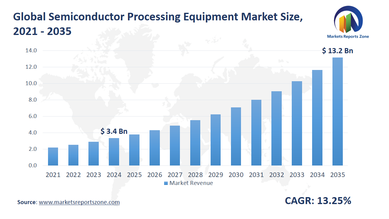
Global Semiconductor Processing Equipment Market Size is expected to reach USD 13.2 Billion by 2035 from USD 3.35 Billion in 2024, with a CAGR of around 13.25% between 2024 and 2035. The global semiconductor processing equipment market has been driven by rising demand for smaller, more efficient electronic devices. Increased adoption of AI, 5G, and IoT technologies has also fueled equipment upgrades. Advanced lithography systems have been deployed in South Korea for next-gen chip production. In Taiwan, high-precision etching machines have been used for manufacturing 3nm chips. However, growth has been restrained by the high cost of machinery and long return on investment. Startups and small fabs have found entry difficult due to capital intensity. Despite this, two major opportunities have been created. First, strong government incentives in countries like India and the U.S. have encouraged new fab construction, boosting demand for processing tools. Second, the expansion of electric vehicles has led to growing use of power semiconductors, opening up new application segments. For instance, specialized deposition systems have been used in Germany for silicon carbide chips in EVs. Also, packaging innovations like 3D stacking have increased interest in advanced bonding and metrology tools. Demand for compact and energy-efficient consumer electronics has kept R&D investments strong. To stay competitive, firms have accelerated automation and AI-based defect inspection systems. As a result, innovation in processing equipment has remained steady across all key regions.
Driver: Rising Tech Demands Fuel Growth
The rising demand for compact, faster, and more powerful electronic devices has acted as a strong driver for the semiconductor processing equipment market. With consumers expecting high-speed smartphones, smarter appliances, and energy-efficient gadgets, chipmakers have been pushed to adopt advanced manufacturing tools. Newer lithography systems, plasma etchers, and ion implanters have been used to fabricate chips with smaller nodes and better power performance. In Japan, production lines for gaming consoles and smart TVs have been upgraded with newer deposition tools to improve yields. In France, fabs producing industrial automation chips have integrated precision metrology systems to ensure consistent quality. This demand has not just come from consumer electronics but also from sectors like healthcare and aerospace, where sensors and processors need to be more compact and reliable. High-performance computing systems, essential in modern data centers, have led to investments in next-gen wafer cleaning and polishing equipment. Even wearables like smartwatches and fitness bands have pushed foundries to explore new materials and high-density packaging methods. To meet these evolving expectations, equipment manufacturers have intensified R&D in hybrid tools, AI-integrated inspection systems, and modular machines. As digital transformation expands globally, processing equipment demand is expected to remain on a steady upward path.
Key Insights:
- The adoption rate of semiconductor processing equipment in advanced manufacturing facilities is approximately 90%, driven by the need for precision and efficiency in chip production.
- Companies and governments have invested over USD 10 billion in semiconductor processing technologies annually to support advancements in AI, IoT, and 5G technologies.
- The penetration rate of semiconductor processing equipment in the automotive sector is around 40%, reflecting the increasing use of semiconductors in vehicle systems.
- The integration of AI and automation has improved the operational efficiency of semiconductor processing equipment by up to 20%, enabling better defect detection and analysis.
- Semiconductor processing equipment is crucial in various industries, including consumer electronics, telecommunications, and industrial automation, accounting for about 70% of all applications.
- Stricter regulations regarding chip quality have led to a 60% increase in the adoption of advanced semiconductor processing equipment to ensure compliance with international standards.
Segment Analysis:
The semiconductor processing equipment market has been shaped by advancements across various types and applications. Lithography systems have been widely used to create finer and more intricate chip patterns, especially in fabs producing AI processors and high-speed memory modules. Wafer surface conditioning tools have been adopted by chipmakers in Singapore to ensure smooth and defect-free wafers before layering begins. Cleaning processes have been crucial in South Korean facilities, where even microscopic contamination has been known to cause expensive yield losses. On the application side, assembly and packaging have evolved rapidly with the push for miniaturization, especially in devices like AR glasses and biometric sensors. Dicing systems have been upgraded in European plants to cut advanced wafers with higher accuracy and reduced material stress. In the U.S., bonding processes have seen innovation with hybrid bonding and 3D stacking, particularly for processors used in autonomous driving systems. Metrology tools have been increasingly deployed in India’s expanding semiconductor initiatives to measure and maintain performance at the nanoscale level. Together, these segments have played vital roles in enhancing chip performance, reducing production errors, and driving technological breakthroughs in sectors like telecommunications, defense, and consumer electronics across global manufacturing hubs.
Regional Analysis:
In North America, advanced semiconductor processing equipment has been embraced by leading fabs in Arizona and Texas, where significant investments have been made to support AI and electric vehicle chip production. In Europe, countries like Germany and the Netherlands have focused on precision tools for wafer cleaning and metrology, especially for chips used in industrial automation and high-end automotive electronics. The Asia-Pacific region has remained a global leader, with Taiwan and Japan upgrading lithography and bonding technologies to meet the demands of 3nm and 2nm chip production. In South Korea, major players have deployed cutting-edge dicing and packaging systems to accelerate development of memory chips used in data centers. Meanwhile, China has been ramping up domestic manufacturing with newer wafer conditioning and etching tools to reduce dependency on imports. In Latin America, semiconductor equipment usage has grown slowly but steadily, especially in Brazil, where local assembly and testing centers have been using compact, cost-effective tools for niche electronics. In the Middle East & Africa, the market has been in a nascent stage, but pilot semiconductor projects in the UAE have begun utilizing imported processing systems for solar and defense applications. Across all regions, innovation and geopolitical strategy have guided investment in equipment upgrades.
Competitive Scenario:
The semiconductor processing equipment market has witnessed significant advancements driven by collaborations and technological innovations. Tokyo Electron has partnered with Tata Electronics to supply equipment and train personnel for India's inaugural semiconductor fabrication facility in Dholera, Gujarat, and an assembly and test unit in Jagiroad, Assam, marking a pivotal step in establishing a semiconductor ecosystem in India. Advantest has emphasized sustainability and innovation in its Integrated Annual Report 2022, reflecting a commitment to environmental responsibility and technological progress. ASML Holding, despite facing stock fluctuations due to reduced investments from key clients like Intel and Samsung, continues to be the sole producer of advanced extreme ultraviolet lithography machines essential for cutting-edge chip production. Applied Materials has introduced the EPIC Advanced Packaging initiative, aiming to enhance energy-efficient computing through advanced chip packaging technologies. KLA Corporation has expanded its manufacturing capabilities in Singapore, contributing to the development of new semiconductor technologies and offering diverse career opportunities. These developments underscore the industry's focus on strategic partnerships, sustainable practices, and technological innovation to meet the evolving demands of the semiconductor sector.
Semiconductor Processing Equipment Market Report Scope
| Report Attribute | Details |
|---|---|
| Market Size Value in 2024 | USD 3.35 Billion |
| Revenue Forecast in 2035 | USD 13.2 Billion |
| Growth Rate | CAGR of 13.25% from 2025 to 2035 |
| Historic Period | 2021 - 2024 |
| Forecasted Period | 2025 - 2035 |
| Report Coverage | Revenue forecast, company ranking, competitive landscape, growth factors, and trends |
| Regions Covered | North America; Europe; Asia Pacific; Latin America; Middle East & Africa |
| Countries Covered | U.S.; Canada; Mexico, UK; Germany; France; Spain; Italy; Russia; China; Japan; India; South Korea; Australia; Southeast Asia; Brazil; Argentina; Saudi Arabia; UAE; South Africa |
| Key companies profiled | Tokyo Electron; LAM RESEARCH; ASML Holdings; Applied Materials; KLA-Tencor Corporation; Screen Holdings; Teradyne; Advantest; Hitachi High-Technologies; Plasma-Therm |
| Customization | Free report customization (equivalent up to 8 analysts working days) with purchase. Addition or alteration to country, regional & segment scope. |
The Global Semiconductor Processing Equipment Market report is segmented as follows:
By Type,
- Lithography
- Wafer Surface Conditioning
- Cleaning Processes
By Application,
- Assembly & Packaging
- Dicing
- Bonding
- Metrology
By Region,
- North America
- U.S.
- Canada
- Mexico
- Europe
- UK
- Germany
- France
- Spain
- Italy
- Russia
- Rest of Europe
- Asia Pacific
- China
- Japan
- India
- South Korea
- Australia
- Southeast Asia
- Rest of Asia Pacific
- Latin America
- Brazil
- Argentina
- Rest of Latin America
- Middle East & Africa
- Saudi Arabia
- UAE
- South Africa
- Rest of Middle East and Africa
Key Market Players,
- Tokyo Electron
- LAM RESEARCH
- ASML Holdings
- Applied Materials
- KLA-Tencor Corporation
- Screen Holdings
- Teradyne
- Advantest
- Hitachi High-Technologies
- Plasma-Therm
Frequently Asked Questions
Research Objectives
- Proliferation and maturation of trade in the global Semiconductor Processing Equipment Market.
- The market share of the global Semiconductor Processing Equipment Market, supply and demand ratio, growth revenue, supply chain analysis, and business overview.
- Current and future market trends that are influencing the growth opportunities and growth rate of the global Semiconductor Processing Equipment Market.
- Feasibility study, new market insights, company profiles, investment return, market size of the global Semiconductor Processing Equipment Market.
Chapter 1 Semiconductor Processing Equipment Market Executive Summary
- 1.1 Semiconductor Processing Equipment Market Research Scope
- 1.2 Semiconductor Processing Equipment Market Estimates and Forecast (2021-2035)
- 1.2.1 Global Semiconductor Processing Equipment Market Value and Growth Rate (2021-2035)
- 1.2.2 Global Semiconductor Processing Equipment Market Price Trend (2021-2035)
- 1.3 Global Semiconductor Processing Equipment Market Value Comparison, by Type (2021-2035)
- 1.3.1 Lithography
- 1.3.2 Wafer Surface Conditioning
- 1.3.3 Cleaning Processes
- 1.4 Global Semiconductor Processing Equipment Market Value Comparison, by Application (2021-2035)
- 1.4.1 Assembly & Packaging
- 1.4.2 Dicing
- 1.4.3 Bonding
- 1.4.4 Metrology
Chapter 2 Research Methodology
- 2.1 Introduction
- 2.2 Data Capture Sources
- 2.2.1 Primary Sources
- 2.2.2 Secondary Sources
- 2.3 Market Size Estimation
- 2.4 Market Forecast
- 2.5 Assumptions and Limitations
Chapter 3 Market Dynamics
- 3.1 Market Trends
- 3.2 Opportunities and Drivers
- 3.3 Challenges
- 3.4 Market Restraints
- 3.5 Porter's Five Forces Analysis
Chapter 4 Supply Chain Analysis and Marketing Channels
- 4.1 Semiconductor Processing Equipment Supply Chain Analysis
- 4.2 Marketing Channels
- 4.3 Semiconductor Processing Equipment Suppliers List
- 4.4 Semiconductor Processing Equipment Distributors List
- 4.5 Semiconductor Processing Equipment Customers
Chapter 5 COVID-19 & Russia?Ukraine War Impact Analysis
- 5.1 COVID-19 Impact Analysis on Semiconductor Processing Equipment Market
- 5.2 Russia-Ukraine War Impact Analysis on Semiconductor Processing Equipment Market
Chapter 6 Semiconductor Processing Equipment Market Estimate and Forecast by Region
- 6.1 Global Semiconductor Processing Equipment Market Value by Region: 2021 VS 2023 VS 2035
- 6.2 Global Semiconductor Processing Equipment Market Scenario by Region (2021-2023)
- 6.2.1 Global Semiconductor Processing Equipment Market Value Share by Region (2021-2023)
- 6.3 Global Semiconductor Processing Equipment Market Forecast by Region (2024-2035)
- 6.3.1 Global Semiconductor Processing Equipment Market Value Forecast by Region (2024-2035)
- 6.4 Geographic Market Analysis: Market Facts and Figures
- 6.4.1 North America Semiconductor Processing Equipment Market Estimates and Projections (2021-2035)
- 6.4.2 Europe Semiconductor Processing Equipment Market Estimates and Projections (2021-2035)
- 6.4.3 Asia Pacific Semiconductor Processing Equipment Market Estimates and Projections (2021-2035)
- 6.4.4 Latin America Semiconductor Processing Equipment Market Estimates and Projections (2021-2035)
- 6.4.5 Middle East & Africa Semiconductor Processing Equipment Market Estimates and Projections (2021-2035)
Chapter 7 Global Semiconductor Processing Equipment Competition Landscape by Players
- 7.1 Global Top Semiconductor Processing Equipment Players by Value (2021-2023)
- 7.2 Semiconductor Processing Equipment Headquarters and Sales Region by Company
- 7.3 Company Recent Developments, Mergers & Acquisitions, and Expansion Plans
Chapter 8 Global Semiconductor Processing Equipment Market, by Type
- 8.1 Global Semiconductor Processing Equipment Market Value, by Type (2021-2035)
- 8.1.1 Lithography
- 8.1.2 Wafer Surface Conditioning
- 8.1.3 Cleaning Processes
Chapter 9 Global Semiconductor Processing Equipment Market, by Application
- 9.1 Global Semiconductor Processing Equipment Market Value, by Application (2021-2035)
- 9.1.1 Assembly & Packaging
- 9.1.2 Dicing
- 9.1.3 Bonding
- 9.1.4 Metrology
Chapter 10 North America Semiconductor Processing Equipment Market
- 10.1 Overview
- 10.2 North America Semiconductor Processing Equipment Market Value, by Country (2021-2035)
- 10.2.1 U.S.
- 10.2.2 Canada
- 10.2.3 Mexico
- 10.3 North America Semiconductor Processing Equipment Market Value, by Type (2021-2035)
- 10.3.1 Lithography
- 10.3.2 Wafer Surface Conditioning
- 10.3.3 Cleaning Processes
- 10.4 North America Semiconductor Processing Equipment Market Value, by Application (2021-2035)
- 10.4.1 Assembly & Packaging
- 10.4.2 Dicing
- 10.4.3 Bonding
- 10.4.4 Metrology
Chapter 11 Europe Semiconductor Processing Equipment Market
- 11.1 Overview
- 11.2 Europe Semiconductor Processing Equipment Market Value, by Country (2021-2035)
- 11.2.1 UK
- 11.2.2 Germany
- 11.2.3 France
- 11.2.4 Spain
- 11.2.5 Italy
- 11.2.6 Russia
- 11.2.7 Rest of Europe
- 11.3 Europe Semiconductor Processing Equipment Market Value, by Type (2021-2035)
- 11.3.1 Lithography
- 11.3.2 Wafer Surface Conditioning
- 11.3.3 Cleaning Processes
- 11.4 Europe Semiconductor Processing Equipment Market Value, by Application (2021-2035)
- 11.4.1 Assembly & Packaging
- 11.4.2 Dicing
- 11.4.3 Bonding
- 11.4.4 Metrology
Chapter 12 Asia Pacific Semiconductor Processing Equipment Market
- 12.1 Overview
- 12.2 Asia Pacific Semiconductor Processing Equipment Market Value, by Country (2021-2035)
- 12.2.1 China
- 12.2.2 Japan
- 12.2.3 India
- 12.2.4 South Korea
- 12.2.5 Australia
- 12.2.6 Southeast Asia
- 12.2.7 Rest of Asia Pacific
- 12.3 Asia Pacific Semiconductor Processing Equipment Market Value, by Type (2021-2035)
- 12.3.1 Lithography
- 12.3.2 Wafer Surface Conditioning
- 12.3.3 Cleaning Processes
- 12.4 Asia Pacific Semiconductor Processing Equipment Market Value, by Application (2021-2035)
- 12.4.1 Assembly & Packaging
- 12.4.2 Dicing
- 12.4.3 Bonding
- 12.4.4 Metrology
Chapter 13 Latin America Semiconductor Processing Equipment Market
- 13.1 Overview
- 13.2 Latin America Semiconductor Processing Equipment Market Value, by Country (2021-2035)
- 13.2.1 Brazil
- 13.2.2 Argentina
- 13.2.3 Rest of Latin America
- 13.3 Latin America Semiconductor Processing Equipment Market Value, by Type (2021-2035)
- 13.3.1 Lithography
- 13.3.2 Wafer Surface Conditioning
- 13.3.3 Cleaning Processes
- 13.4 Latin America Semiconductor Processing Equipment Market Value, by Application (2021-2035)
- 13.4.1 Assembly & Packaging
- 13.4.2 Dicing
- 13.4.3 Bonding
- 13.4.4 Metrology
Chapter 14 Middle East & Africa Semiconductor Processing Equipment Market
- 14.1 Overview
- 14.2 Middle East & Africa Semiconductor Processing Equipment Market Value, by Country (2021-2035)
- 14.2.1 Saudi Arabia
- 14.2.2 UAE
- 14.2.3 South Africa
- 14.2.4 Rest of Middle East & Africa
- 14.3 Middle East & Africa Semiconductor Processing Equipment Market Value, by Type (2021-2035)
- 14.3.1 Lithography
- 14.3.2 Wafer Surface Conditioning
- 14.3.3 Cleaning Processes
- 14.4 Middle East & Africa Semiconductor Processing Equipment Market Value, by Application (2021-2035)
- 14.4.1 Assembly & Packaging
- 14.4.2 Dicing
- 14.4.3 Bonding
- 14.4.4 Metrology
Chapter 15 Company Profiles and Market Share Analysis: (Business Overview, Market Share Analysis, Products/Services Offered, Recent Developments)
- 15.1 Tokyo Electron
- 15.2 LAM RESEARCH
- 15.3 ASML Holdings
- 15.4 Applied Materials
- 15.5 KLA-Tencor Corporation
- 15.6 Screen Holdings
- 15.7 Teradyne
- 15.8 Advantest
- 15.9 Hitachi High-Technologies
- 15.10 Plasma-Therm
Report ID:
126
Published Date:
April 2025
Trusted by more than 10,500 organizations globally


Infaluble Methodology
Customization
Analyst Support
Targeted Market View